| Version 25 (modified by murphpo, 15 years ago) (diff) |
|---|
WARP FPGA Board MGTs
The Virtex-4 FPGA is equipped with 10 pairs of differential multi-gigabit transceivers. Each MGT is a full-duplex transceiver supporting serial data rates up to 6.5 Gbps. The WARP FPGA board includes 8 MGT interfaces: 4 HSSDC2, 2 SATA and 2 SFP.
The MGTs on the Virtex-4 FPGA are internally organized in two columns. Each column has two clock inputs and all the MGTs in the column can use either of those clocks. Our design maximizes the functionality by allowing the user to select the clock frequency that is input to the columns.
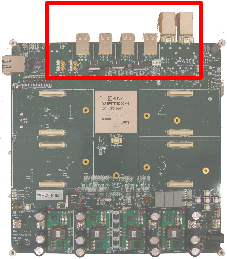
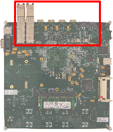
All the MGT connectors are located on the north side of the FPGA Board; both on the top and bottom.
MGT Connectors
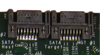
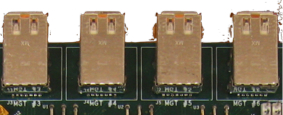
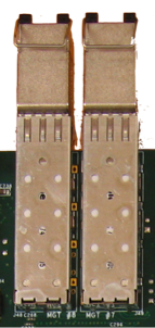
There are three types of MGT connectors on the board. Two Small form-factor Pluggable (SFP) are connected to one column in the FPGA. The HSSDC2 and SATA interfaces are connected to the other column.
 |  | 
|
| SATA Interfaces | HSSDC2 Interfaces | SFP Interfaces |
The MGT interfaces are labeled "MGT 1" to "MGT 8" on the WARP FPGA board. The table below shows the mapping of each interface to the corresponding MGT in the FPGA.
| MGT # | Type | Connector | MGT Tile | Column | LOC Constraint | TXP | TXN | RXP | RXN | Ideal Clocks |
| 1 | SATA Target | J47 | 112B | 1 | GT11_X1Y4 | P1 | R1 | U1 | V1 | MGTCLK_110 or MGTCLK_113 |
| 2 | SATA Host | J46 | 112A | 1 | GT11_X1Y5 | M1 | N1 | J1 | K1 | MGTCLK_110 or MGTCLK_113 |
| 3 | HSSDC2 | J3 | 113B | 1 | GT11_X1Y6 | A4 | A3 | C1 | D1 | MGTCLK_110 or MGTCLK_113 |
| 4 | HSSDC2 | J4 | 113A | 1 | GT11_X1Y7 | A6 | A5 | A9 | A8 | MGTCLK_110 or MGTCLK_113 |
| 5 | HSSDC2 | J5 | 114B | 1 | GT11_X1Y8 | A14 | A13 | A11 | A10 | MGTCLK_110 or MGTCLK_113 |
| 6 | HSSDC2 | J6 | 114A | 1 | GT11_X1Y9 | A16 | A15 | A19 | A18 | MGTCLK_110 or MGTCLK_113 |
| 7 | SFP #1 | J49 | 102A | 0 | GT11_X0Y7 | A34 | A35 | A31 | A32 | MGTCLK_102 or MGTCLK_105 |
| 8 | SFP #2 | J48 | 102B | 0 | GT11_X0Y6 | A36 | A37 | C39 | D39 | MGTCLK_102 or MGTCLK_105 |
MGT Clocking
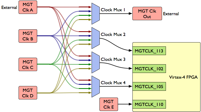
THe WARP FPGA Board provides very flexible MGT clocking. The Virtex-4 FPGA organizes the MGTs into two columns. Each column provides two clock inputs. Each MGT can use either clock driven into its column As mentioned, each MGT column has two input clocks that are shared. Any of the MGT tiles in that column share the clocks. In column 0 the clock inputs are located at tile 102 and tile 105. In column 1, the inputs are tile 10 and tile 13. There is an elaborate clock multiplexer scheme on the board that lets the user choose three of the four clock inputs.
MGT Clock Sources
| Clock Source | Component | Mux Input | Source |
| MGT Clk A | J14 or J11/J18 | 0 | Off Board Connectors |
| MGT Clk B | Y2 | 1 | Oscillator (Not Installed) |
| MGT Clk C | Y3 | 2 | 250MHz Oscillator |
| MGT Clk D | Y4 | 3 | Oscillator (Not Installed) |
| MGT Clk E | Y8 | - | 300MHz Oscillator |
FPGA MGT Clock Inputs
| Clock Input | Tile | Column | GT11CLK LOC | P Pin | N Pin | Source |
| MGTCLK_102 | 102 | 0 | GT11CLK_X0Y3 | F39 | G39 | Mux 3 |
| MGTCLK_105 | 105 | 0 | GT11CLK_X0Y1 | AW34 | AW33 | Mux 4 |
| MGTCLK_110 | 110 | 1 | GT11CLK_X1Y1 | AW6 | AW7 | MGT Clk E (Y8) |
| MGTCLK_113 | 113 | 1 | GT11CLK_X1Y3 | F1 | G1 | Mux 2 |

External clock input and output (top of the FPGA Board)
There are four clock multiplexers on the board with four inputs each. The four possible inputs are MGT Clk A (external clock), MGT Clk B (NM), MGT Clk C (250 MHz) and MGT Clk D (NM). Mux1 is used to source another board, especially useful for sharing clocks between boards. The other three multiplexers source one of the FPGA Clock inputs. As there are four inputs, two bits are required to control every mux. Two 4-input dip switches choose the output of every mux.

Multiplexer output select switches (bottom of the FPGA Board)
The following table details the value required for each bit of SW10 and SW11 to obtain the desired output.
| MGT Clk A | MGT Clk B | MGT Clk C | MGT Clk D | SW/Bit | |
| Mux1 |  |  |  |  | SW10, Bits 2 and 3 |
| Mux2 |  |  |  |  | SW10, Bits 0 and 1 |
| Mux3 |  |  |  |  | SW11, Bits 2 and 3 |
| Mux4 |  |  |  |  | SW11, Bits 0 and 1 |
More information regarding MGT designs is included in Xilinx documentation (MGT User Guide).
Connectors & Cables
Four MGTs are wired to Infiniband-keyed HSSDC2 jacks. You must use an Infiniband-keyed 100Ω HSDDC2-HSDDC2 cable to connect two FPGA boards together. One such cable is made by Molex (Molex HSDDC2 Cables).
The two SFP connectors require an additional module to connect Ethernet cables. Molex creates one such module supported by the FPGA.
